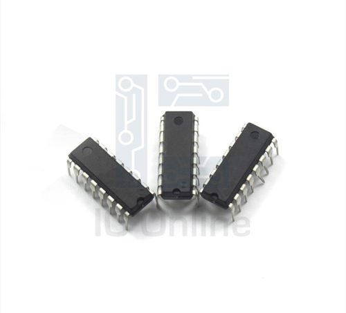
JANKCB2N2221A-Transistor-Die Overview
The JANKCB2N2221A transistor die is a high-performance NPN bipolar junction transistor designed for general-purpose amplification and switching applications. Featuring robust electrical characteristics and reliable gain performance, this transistor die is ideal for integration into discrete semiconductor packages or hybrid modules. Its compact die structure supports efficient thermal dissipation and enhanced switching speeds, making it suitable for industrial and consumer electronics use cases. With stable operation under varied conditions, this transistor die meets the rigorous demands of modern electronic designs. For more detailed information, visit IC Manufacturer.
JANKCB2N2221A-Transistor-Die Technical Specifications
| Parameter | Specification |
|---|---|
| Type | NPN Bipolar Junction Transistor |
| Maximum Collector-Emitter Voltage (VCEO) | 40 V |
| Maximum Collector Current (IC) | 600 mA |
| Transition Frequency (fT) | 300 MHz |
| DC Current Gain (hFE) | 100 to 300 |
| Power Dissipation (PD) | 500 mW (die level) |
| Package Type | Transistor Die (bare semiconductor die) |
| Operating Temperature Range | -55??C to +150??C |
JANKCB2N2221A-Transistor-Die Key Features
- High Transition Frequency: Supports up to 300 MHz for fast switching, enabling improved performance in RF and high-speed circuits.
- Robust Current Handling: Collector current rating up to 600 mA allows reliable operation in moderate power amplification and switching roles.
- Wide Operating Temperature Range: Ensures stable transistor functionality from -55??C to +150??C, suitable for harsh industrial environments.
- Compact Bare Die Form: Enables flexible integration into custom hybrid modules or advanced packaging, reducing parasitic effects and enhancing thermal performance.
Typical Applications
- General-purpose amplification in signal processing circuits, offering dependable gain and frequency response for audio or intermediate frequency applications.
- Switching elements in industrial control systems requiring fast response and robust current capacity.
- Driver stages in low to medium power electronic devices where compact transistor dies enable space-saving designs.
- Integration in hybrid analog circuits and multi-chip modules needing bare die components for optimized electrical and thermal characteristics.
JANKCB2N2221A-Transistor-Die Advantages vs Typical Alternatives
This transistor die delivers a combination of high gain, fast switching frequency, and wide temperature tolerance that enhances reliability and performance compared to typical discrete transistors. Its bare die format allows better thermal management and customized packaging integration, reducing parasitic capacitances and improving efficiency. These advantages make it a preferred choice for engineers seeking compact, robust transistor solutions in demanding industrial and signal amplification applications.
🔥 Best-Selling Products
-
Texas Instruments BQ24075 Linear Battery Charger IC – 5mm x 4mm QFN Package
-

Texas Instruments INA219 Current Sensor Module – SOIC Package, Precision Monitoring
-

Texas Instruments LM4041 Precision Voltage Reference – SOT-23 Package
-

Texas Instruments OPA2134 Audio Op Amp – Dual, High-Performance, SOIC-8 Package
JANKCB2N2221A-Transistor-Die Brand Info
The JANKCB2N2221A transistor die is part of the renowned 2N2221 transistor family, widely recognized and manufactured by established semiconductor producers specializing in discrete components. This device is typically supplied by semiconductor manufacturers who provide bare die formats for custom assembly and integration. The transistor??s heritage traces back to industry-standard designs known for reliability and versatile performance in amplification and switching tasks. Engineers sourcing this die benefit from the proven track record of the 2N2221 transistor lineage adapted to modern bare die applications.
FAQ
What is the maximum voltage rating of this transistor die?
The maximum collector-emitter voltage (VCEO) for this transistor die is 40 volts, ensuring safe operation within most low to medium voltage amplifier and switching circuits.
🌟 Featured Products
-

“Buy MAX9312ECJ+ Precision Voltage Comparator in DIP Package for Reliable Performance”
-
QCC-711-1-MQFN48C-TR-03-1 Bluetooth Audio SoC with MQFN48C Package
-

0339-671-TLM-E Model – High-Performance TLM-E Package for Enhanced Functionality
-
1-1415898-4 Connector Housing, Electrical Wire-to-Board, Receptacle, Packaged
Can this transistor die handle high-frequency signals?
Yes, the transistor die supports transition frequencies up to 300 MHz, making it suitable for high-speed switching and RF amplification in applications requiring fast response times.


