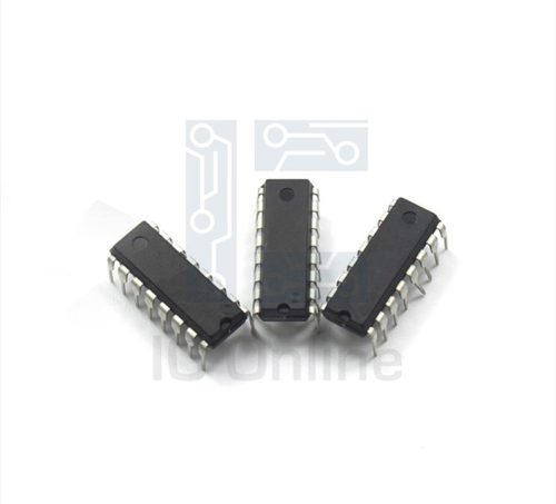
JANKCBM2N2222A-Transistor-Die Overview
The JANKCBM2N2222A-Transistor-Die is a high-performance NPN bipolar junction transistor die designed for amplification and switching applications in industrial and electronic systems. This transistor die offers reliable current gain with excellent switching speed and moderate power dissipation, making it suitable for a wide range of analog and digital circuits. Its die form factor allows for integration into custom semiconductor packages or specialized circuit modules. Engineers and sourcing specialists will appreciate its consistent electrical characteristics and compatibility with standard transistor applications. For quality assurance and supply chain reliability, visit IC Manufacturer.
JANKCBM2N2222A-Transistor-Die Technical Specifications
| Parameter | Value |
|---|---|
| Transistor Type | NPN Bipolar Junction Transistor (BJT) |
| Maximum Collector-Emitter Voltage (Vce) | 40 V |
| Maximum Collector Current (Ic) | 600 mA |
| DC Current Gain (hFE) | 100 to 300 (typical at Ic = 150 mA) |
| Transition Frequency (fT) | 300 MHz (typical) |
| Power Dissipation (Pd) | 625 mW (die level, subject to packaging and mounting) |
| Base-Emitter Voltage (Vbe) | Approximately 0.7 V (typical) |
| Package Type | Transistor Die (bare silicon die) |
| Operating Temperature Range | -55??C to +150??C |
JANKCBM2N2222A-Transistor-Die Key Features
- High-Speed Switching: Enables fast switching times up to 300 MHz, critical for efficient signal processing in complex circuits.
- Robust Current Gain: Provides stable current amplification with a typical gain range of 100?C300, ensuring reliable performance in amplification tasks.
- Thermal Stability: Operates effectively across a wide temperature range, enhancing reliability in harsh industrial environments.
- Die-Level Flexibility: Allows custom packaging or integration, giving designers freedom for specialized applications and compact form factors.
Typical Applications
- General-purpose low-power amplification circuits, including audio preamplifiers and signal conditioning modules requiring consistent gain and low noise.
- Switching applications in industrial control systems where fast response and reliable operation are essential.
- Driver stages for relays, LEDs, and small motors in embedded electronics and automation equipment.
- Complementary transistor arrays or hybrid integrated circuits where custom die integration enhances circuit density.
JANKCBM2N2222A-Transistor-Die Advantages vs Typical Alternatives
This transistor die offers a blend of moderate power handling, high current gain, and fast switching speed that surpasses many generic NPN transistor dies. Its bare die format provides integration flexibility unmatched by packaged alternatives, enabling optimized circuit layouts and enhanced thermal management. Additionally, the die??s stable electrical characteristics and wide operating temperature range support improved reliability and performance in demanding industrial applications.
🔥 Best-Selling Products
-
Texas Instruments BQ24075 Linear Battery Charger IC – 5mm x 4mm QFN Package
-

Texas Instruments INA219 Current Sensor Module – SOIC Package, Precision Monitoring
-

Texas Instruments LM4041 Precision Voltage Reference – SOT-23 Package
-

Texas Instruments OPA2134 Audio Op Amp – Dual, High-Performance, SOIC-8 Package
JANKCBM2N2222A-Transistor-Die Brand Info
The JANKCBM2N2222A-Transistor-Die is manufactured by JANKC Semiconductor, a trusted supplier specializing in discrete semiconductor components tailored for industrial and commercial electronics markets. The company is known for delivering reliable transistor dies with precise electrical characteristics and consistent quality control. JANKC??s product line includes a wide range of bipolar junction transistor dies designed for robust performance in amplification, switching, and signal processing roles. This specific transistor die benefits from JANKC??s advanced fabrication processes, ensuring high yield and stable operation across varied environments.
FAQ
What is the maximum collector current rating for this transistor die?
The maximum collector current rating is 600 mA. This rating defines the highest continuous current the transistor die can handle safely under specified operating conditions without damage.
🌟 Featured Products
-

“Buy MAX9312ECJ+ Precision Voltage Comparator in DIP Package for Reliable Performance”
-
QCC-711-1-MQFN48C-TR-03-1 Bluetooth Audio SoC with MQFN48C Package
-

0339-671-TLM-E Model – High-Performance TLM-E Package for Enhanced Functionality
-
1-1415898-4 Connector Housing, Electrical Wire-to-Board, Receptacle, Packaged
Can this transistor die be used for high-frequency applications?
Yes, the transistor die has a typical transition frequency of approximately 300 MHz, making it suitable for moderate to high-frequency switching and amplification tasks in analog and digital circuits.
What are the thermal operating limits for the transistor die?
The operating


