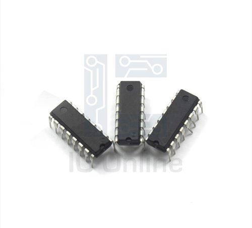
JANTXV2N3838-Dual-Transistor Overview
The JANTXV2N3838 Dual Transistor is a high-reliability, matched NPN transistor pair designed for precision amplification and switching applications. Constructed to meet stringent military standards, it offers excellent gain linearity and thermal stability, ensuring consistent performance under demanding conditions. This device is ideal for use in instrumentation, control circuits, and other industrial electronics where dependable operation is critical. Manufactured following IC Manufacturer??s rigorous quality protocols, it guarantees long service life and robust electrical characteristics.
JANTXV2N3838-Dual-Transistor Technical Specifications
| Parameter | Specification |
|---|---|
| Transistor Type | NPN Dual Matched Pair |
| Collector-Emitter Voltage (VCEO) | 30 V |
| Collector-Base Voltage (VCBO) | 40 V |
| Emitter-Base Voltage (VEBO) | 5 V |
| Collector Current (IC) | 200 mA |
| Power Dissipation (Ptot) | 625 mW |
| Current Gain (hFE) at IC = 2 mA | 70 to 700 |
| Transition Frequency (fT) | 100 MHz (typical) |
| Package | TO-18 Metal Can |
JANTXV2N3838-Dual-Transistor Key Features
- Matched transistor pair: Ensures precise gain matching for differential amplifier circuits, improving signal integrity and reducing distortion.
- Wide voltage ratings: Supports up to 40 V collector-base voltage, offering flexibility in various circuit designs including moderate power switching.
- High gain range: Provides hFE values from 70 to 700, allowing designers to select operating points for optimal linearity or amplification.
- Robust packaging: The TO-18 metal can package enhances thermal dissipation and mechanical durability for reliable operation in harsh environments.
Typical Applications
- Precision differential amplifiers used in instrumentation systems requiring matched transistor pairs for accurate signal processing and low noise.
- Current mirror circuits benefiting from the matched gain and thermal tracking of the transistor pair to maintain stable reference currents.
- Switching circuits in control systems where reliable transistor operation at moderate voltage and current levels is critical.
- Signal processing modules in industrial electronics, where thermal stability and gain consistency are essential for performance.
JANTXV2N3838-Dual-Transistor Advantages vs Typical Alternatives
This dual transistor pair offers superior gain matching and thermal tracking compared to discrete transistor alternatives, enhancing circuit accuracy and stability. Its rugged TO-18 package provides better heat dissipation and mechanical protection, improving reliability in industrial environments. The wide voltage and current ratings enable versatile use in various control and amplification applications, making it a preferred choice for engineers prioritizing precision and durability.
🔥 Best-Selling Products
-
Texas Instruments BQ24075 Linear Battery Charger IC – 5mm x 4mm QFN Package
-

Texas Instruments INA219 Current Sensor Module – SOIC Package, Precision Monitoring
-

Texas Instruments LM4041 Precision Voltage Reference – SOT-23 Package
-

Texas Instruments OPA2134 Audio Op Amp – Dual, High-Performance, SOIC-8 Package
JANTXV2N3838-Dual-Transistor Brand Info
The JANTXV2N3838 is a military-grade transistor pair produced under strict quality controls by established semiconductor manufacturers specializing in high-reliability components. This product line is known for compliance with JAN (Joint Army-Navy) standards, which certify devices for use in defense and aerospace applications. The brand emphasizes durability, consistent electrical performance, and long-term availability, ensuring that engineers sourcing this component can rely on its proven track record within critical industrial and military systems.
FAQ
What does the ??Dual Transistor?? configuration mean for this device?
The dual transistor configuration means that two matched NPN transistors are integrated within a single package. This allows for closely matched electrical characteristics such as gain and leakage currents, which is essential for differential and current mirror circuits requiring precise matching and consistent performance.
🌟 Featured Products
-

“Buy MAX9312ECJ+ Precision Voltage Comparator in DIP Package for Reliable Performance”
-
QCC-711-1-MQFN48C-TR-03-1 Bluetooth Audio SoC with MQFN48C Package
-

0339-671-TLM-E Model – High-Performance TLM-E Package for Enhanced Functionality
-
1-1415898-4 Connector Housing, Electrical Wire-to-Board, Receptacle, Packaged
What are the typical operating voltage limits for this transistor pair?
This device supports a maximum collector-base voltage of 40 V and a collector-emitter voltage of 30 V, making it suitable for moderate-voltage applications. The emitter-base voltage is limited to


