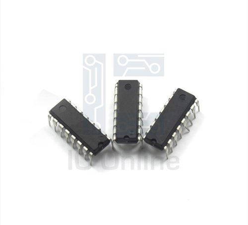
JANKCCL2N5151-Transistor-Die Overview
The JANKCCL2N5151-Transistor-Die is a high-performance semiconductor component designed for precise amplification and switching applications. This transistor die offers robust electrical characteristics, including a maximum collector current of 1.5A and a collector-emitter voltage rating of 120V, making it suitable for medium-power circuits. Its compact die format allows seamless integration into custom semiconductor packages or modules. The device ensures reliable operation with a maximum power dissipation of 30W, supporting efficient thermal management. Ideal for industrial electronics and power control solutions, this transistor die delivers consistent performance under demanding conditions. Available through IC Manufacturer, it supports advanced design flexibility for engineers and sourcing specialists.
JANKCCL2N5151-Transistor-Die Technical Specifications
| Parameter | Specification |
|---|---|
| Collector-Emitter Voltage (Vce) | 120 V |
| Collector Current (Ic) | 1.5 A |
| Power Dissipation (Pd) | 30 W |
| DC Current Gain (hFE) | 40 to 320 |
| Transition Frequency (fT) | 30 MHz |
| Emitter-Base Voltage (Veb) | 5 V |
| Collector-Base Voltage (Vcb) | 120 V |
| Junction Temperature (Tj) | 150 ??C |
JANKCCL2N5151-Transistor-Die Key Features
- High voltage rating: Supports up to 120V collector-emitter voltage, enabling operation in medium-voltage applications with enhanced durability.
- Robust current capacity: 1.5A maximum collector current ensures effective handling of moderate power levels without compromising reliability.
- Wide current gain range: DC current gain between 40 and 320 provides design flexibility for amplification and switching tasks.
- Compact die format: Facilitates integration into custom semiconductor packages or power modules, optimizing space in complex circuits.
- High transition frequency: 30 MHz frequency capability supports fast switching and high-speed signal processing.
- Thermal endurance: Maximum junction temperature of 150??C allows stable operation under demanding thermal conditions.
Typical Applications
- Power switching circuits: The transistor die is ideal for switching applications in medium-power electronic devices, providing reliable control and amplification.
- Amplifier stages: Suitable for linear amplification in audio, industrial, and communication equipment requiring consistent gain performance.
- Motor control systems: Effective in controlling DC motors and actuators where voltage and current demands align with its specifications.
- Custom semiconductor modules: Enables engineers to design tailored power devices by integrating the die within bespoke packaging solutions.
JANKCCL2N5151-Transistor-Die Advantages vs Typical Alternatives
This transistor die offers a competitive edge over typical alternatives through its balanced voltage and current ratings combined with a broad current gain spectrum. Its compact die design allows for efficient packaging and integration, enhancing overall device reliability and thermal management. The high transition frequency supports applications requiring fast switching speeds, while the robust junction temperature rating ensures stable operation in harsh environments, making it a versatile choice for industrial-grade electronics.
🔥 Best-Selling Products
-
Texas Instruments BQ24075 Linear Battery Charger IC – 5mm x 4mm QFN Package
-

Texas Instruments INA219 Current Sensor Module – SOIC Package, Precision Monitoring
-

Texas Instruments LM4041 Precision Voltage Reference – SOT-23 Package
-

Texas Instruments OPA2134 Audio Op Amp – Dual, High-Performance, SOIC-8 Package
JANKCCL2N5151-Transistor-Die Brand Info
The JANKCCL2N5151-Transistor-Die is manufactured by JANKCC, a recognized provider of semiconductor components specializing in transistor dies and discrete devices. The brand focuses on delivering high-quality, reliable semiconductor products designed to meet the rigorous demands of industrial and power electronics markets. JANKCC emphasizes precision manufacturing and rigorous testing to ensure consistent performance and durability in their transistor dies, supporting engineers and sourcing specialists in creating optimized electronic solutions.
FAQ
What are the primary electrical limits of the JANKCCL2N5151 transistor die?
The transistor die supports a maximum collector-emitter voltage of 120V and a collector current rating of up to 1.5A. It
🌟 Featured Products
-

“Buy MAX9312ECJ+ Precision Voltage Comparator in DIP Package for Reliable Performance”
-
QCC-711-1-MQFN48C-TR-03-1 Bluetooth Audio SoC with MQFN48C Package
-

0339-671-TLM-E Model – High-Performance TLM-E Package for Enhanced Functionality
-
1-1415898-4 Connector Housing, Electrical Wire-to-Board, Receptacle, Packaged


