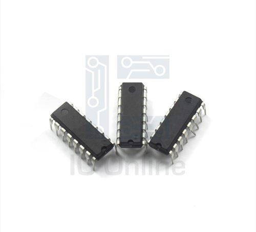
JANTXV2N5664P-Transistor-PIND Overview
The JANTXV2N5664P is a high-performance transistor designed for precision switching and amplification in industrial and military-grade applications. This transistor features a robust design with stringent screening per JAN standards, ensuring superior reliability and stability under demanding conditions. With its complementary PNP configuration, it supports effective current gain and voltage handling, making it ideal for use in complex electronic circuits. Engineered to meet rigorous quality requirements, this device is optimized for longevity and consistent electrical performance. For detailed sourcing and product inquiries, refer to IC Manufacturer.
JANTXV2N5664P-Transistor-PIND Key Features
- High Current Gain: Offers efficient signal amplification, improving circuit sensitivity and response.
- JAN Screening Compliance: Meets military-grade standards, ensuring enhanced reliability and durability in harsh environments.
- Low Noise Operation: Supports clean switching and amplification, critical for precision electronics.
- Robust Package Design: Provides superior thermal dissipation and mechanical stability for sustained performance.
JANTXV2N5664P-Transistor-PIND Technical Specifications
| Parameter | Specification |
|---|---|
| Type | PNP Bipolar Junction Transistor |
| Collector-Emitter Voltage (Vce) | 60 V |
| Collector Current (Ic) | 600 mA |
| Power Dissipation (Ptot) | 800 mW |
| DC Current Gain (hFE) | 40 to 300 |
| Transition Frequency (fT) | 100 MHz |
| Operating Temperature Range | -55??C to +125??C |
| Package Type | Plastic Induction Device (PIND) Package |
JANTXV2N5664P-Transistor-PIND Advantages vs Typical Alternatives
This transistor provides superior reliability and tighter parameter control compared to standard commercial types. Its JAN screening ensures consistent operation in extreme temperature and voltage conditions, making it ideal for mission-critical applications. The combination of high current gain and low noise improves circuit efficiency and signal integrity, providing a dependable solution where precision and durability are paramount.
🔥 Best-Selling Products
-
Texas Instruments BQ24075 Linear Battery Charger IC – 5mm x 4mm QFN Package
-

Texas Instruments INA219 Current Sensor Module – SOIC Package, Precision Monitoring
-

Texas Instruments LM4041 Precision Voltage Reference – SOT-23 Package
-

Texas Instruments OPA2134 Audio Op Amp – Dual, High-Performance, SOIC-8 Package
Typical Applications
- Precision analog signal amplification in aerospace and military electronic systems requiring highly reliable components with stringent quality standards.
- Switching elements in industrial control circuits where robustness and thermal stability are critical for operational longevity.
- Low noise amplifier stages in communication equipment, enhancing overall signal clarity and system performance.
- Complementary transistor pairs in analog and digital interface circuits requiring matched PNP configurations.
JANTXV2N5664P-Transistor-PIND Brand Info
The JANTXV2N5664P transistor is part of the JAN (Joint Army-Navy) series, known for military-grade screening and testing processes. This brand specializes in delivering components that meet strict performance and reliability criteria suitable for defense, aerospace, and high-reliability industrial applications. The product is built to comply with rigorous standards, ensuring consistent electrical characteristics and extended service life under harsh conditions.
FAQ
What does the JAN screening certification mean for this transistor?
JAN screening certifies that the transistor has undergone extensive testing for reliability, including temperature cycling, burn-in, and electrical parameter verification. This ensures the device performs consistently in demanding environments, meeting military and aerospace quality standards.
🌟 Featured Products
-

“Buy MAX9312ECJ+ Precision Voltage Comparator in DIP Package for Reliable Performance”
-
QCC-711-1-MQFN48C-TR-03-1 Bluetooth Audio SoC with MQFN48C Package
-

0339-671-TLM-E Model – High-Performance TLM-E Package for Enhanced Functionality
-
1-1415898-4 Connector Housing, Electrical Wire-to-Board, Receptacle, Packaged
What are the key electrical limits of this transistor?
The transistor supports a maximum collector-emitter voltage of 60 V, collector current up to 600 mA, and power dissipation of 800 mW. It operates reliably within a temperature range from -55??C to +125??C, suitable for harsh environments.
How does the PIND package benefit the device’s performance?
The Plastic Induction Device (PIND) package offers enhanced mechanical protection and improved thermal dissipation, which helps maintain stable operation and prolongs the transistor??s lifespan under continuous use and temperature variations.
📩 Contact Us
In what kind of circuits is this transistor typically used?
This transistor is commonly used in analog amplification, switching, and interface circuits where high gain, low noise, and reliability are required. It is especially suited for military, aerospace, and industrial control applications.
Can this transistor be used in high-frequency applications?
Yes, with a transition frequency (fT) of approximately 100 MHz, it is suitable for moderate high-frequency applications, including RF amplifiers and signal processing circuits requiring reliable PNP transistor performance.


