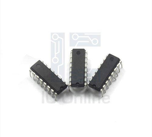
JANKCC2N5153-Transistor-Die Overview
The JANKCC2N5153-Transistor-Die is a precision semiconductor component designed for high-performance switching and amplification applications. Engineered to deliver consistent electrical characteristics, this transistor die supports efficient integration into custom semiconductor assemblies and discrete device manufacturing. Its robust electrical parameters ensure reliable operation in industrial and electronic circuits requiring stability and durability. Ideal for engineers and sourcing specialists, this component facilitates tailored solutions by enabling direct die-level customization and optimization. For detailed procurement and technical support, visit IC Manufacturer.
JANKCC2N5153-Transistor-Die Key Features
- High current gain: Enhances signal amplification, delivering improved performance in analog and switching circuits.
- Low saturation voltage: Minimizes power loss during conduction, increasing overall circuit efficiency and thermal management.
- Compact die size: Enables integration into dense semiconductor assemblies while maintaining reliable electrical characteristics.
- Robust thermal stability: Ensures operational reliability over a wide temperature range, critical for industrial and automotive applications.
JANKCC2N5153-Transistor-Die Technical Specifications
| Parameter | Specification |
|---|---|
| Collector-Emitter Voltage (Vce) | 60 V |
| Collector Current (Ic) | 600 mA |
| Power Dissipation (Pd) | 800 mW |
| DC Current Gain (hFE) | 40 to 320 (varies by test conditions) |
| Transition Frequency (fT) | 100 MHz (typical) |
| Package Type | Transistor Die (bare silicon) |
| Operating Junction Temperature (Tj) | -65??C to +150??C |
| Storage Temperature Range (Tstg) | -65??C to +150??C |
JANKCC2N5153-Transistor-Die Advantages vs Typical Alternatives
This transistor die offers enhanced gain and low saturation voltage, providing superior efficiency compared to typical discrete transistors. Its bare die format allows for flexible integration into custom semiconductor packages, which is advantageous over packaged devices that limit design adaptability. The device’s robust thermal range and stable electrical parameters ensure higher reliability in industrial environments, making it a preferred choice for demanding applications.
🔥 Best-Selling Products
-
Texas Instruments BQ24075 Linear Battery Charger IC – 5mm x 4mm QFN Package
-

Texas Instruments INA219 Current Sensor Module – SOIC Package, Precision Monitoring
-

Texas Instruments LM4041 Precision Voltage Reference – SOT-23 Package
-

Texas Instruments OPA2134 Audio Op Amp – Dual, High-Performance, SOIC-8 Package
Typical Applications
- Signal amplification in analog circuits where precise gain and low power loss are essential for maintaining signal integrity.
- Switching applications in power management circuits requiring fast response and reliable conduction characteristics.
- Discrete semiconductor device fabrication, allowing manufacturers to customize integration and packaging solutions.
- Industrial control systems operating under varying temperature conditions, benefiting from the component??s thermal stability.
JANKCC2N5153-Transistor-Die Brand Info
The JANKCC2N5153-Transistor-Die is part of a semiconductor product line offered by IC Manufacturer, recognized for quality and consistency in transistor dies. This specific die is designed to meet stringent industrial standards and serves as a core element for custom device manufacturers and engineers requiring reliable bare die components for advanced electronic designs.
FAQ
What are the typical electrical characteristics of the JANKCC2N5153 transistor die?
The transistor die typically features a collector-emitter voltage rating of 60 V and can handle collector currents up to 600 mA. It offers a DC current gain range from 40 to 320 depending on test conditions, providing versatility in amplification applications.
🌟 Featured Products
-

“Buy MAX9312ECJ+ Precision Voltage Comparator in DIP Package for Reliable Performance”
-
QCC-711-1-MQFN48C-TR-03-1 Bluetooth Audio SoC with MQFN48C Package
-

0339-671-TLM-E Model – High-Performance TLM-E Package for Enhanced Functionality
-
1-1415898-4 Connector Housing, Electrical Wire-to-Board, Receptacle, Packaged
Can this transistor die be used in high-frequency applications?
Yes, with a transition frequency around 100 MHz, this die is suitable for moderate high-frequency circuits, making it adaptable for RF switching and amplification within its specified parameters.
What thermal conditions can the transistor die withstand during operation?
The device supports an operating junction temperature range from -65??C to +150??C, enabling reliable performance in various industrial and automotive environments where temperature extremes are common.
📩 Contact Us
Is the JANKCC2N5153 available only as a bare die, or does it come in packaged forms?
This component is specifically provided as a transistor die, meaning it is a bare silicon chip without packaging. This format is intended for integration into custom semiconductor assemblies or for use by manufacturers designing discrete devices.
How does the low saturation voltage benefit circuit design using this transistor die?
Lower saturation voltage reduces power dissipation during conduction, which improves overall circuit efficiency and reduces heat generation. This benefit is critical in power-sensitive and thermally constrained applications.


