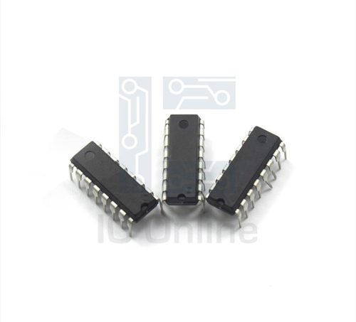
2N5115-JFET-PChannel Overview
The 2N5115 is a P-Channel Junction Field Effect Transistor (JFET) designed for high-voltage, low-noise analog switching and amplification applications. Known for its robust electrical characteristics and reliable performance, it operates efficiently with a maximum drain-source voltage rating suitable for demanding circuits. This device offers excellent input impedance and low gate leakage, making it ideal for precision analog signal processing. Engineers and sourcing specialists can leverage this component for enhanced analog circuit design, benefiting from its stable operation and consistent parameters. For more detailed sourcing and specifications, visit IC Manufacturer.
2N5115-JFET-PChannel Key Features
- High Voltage Handling: Supports up to 60 V drain-source voltage, enabling use in circuits requiring robust voltage tolerance.
- Low Noise Operation: Minimizes signal distortion, critical for sensitive analog and audio applications.
- High Input Impedance: Ensures minimal loading on preceding circuit stages, preserving signal integrity.
- Reliable Thermal Performance: Designed for stable operation with a maximum power dissipation of 310 mW, enhancing circuit longevity.
2N5115-JFET-PChannel Technical Specifications
| Parameter | Value | Unit |
|---|---|---|
| Drain-Source Voltage (V_DS) | 60 | V |
| Gate-Source Voltage (V_GS) | -30 | V |
| Continuous Drain Current (I_D) | -100 | mA |
| Power Dissipation (P_D) | 310 | mW |
| Gate Reverse Current (I_GSS) | -100 | nA |
| Zero Gate Voltage Drain Current (I_DSS) | -1 | mA |
| Gate Threshold Voltage (V_GS(off)) | -0.5 to -6 | V |
| Transition Frequency (f_T) | 5 | MHz |
2N5115-JFET-PChannel Advantages vs Typical Alternatives
This P-Channel JFET offers superior voltage handling and low noise characteristics compared to many general-purpose transistors. Its high input impedance and low gate leakage current provide precise control in analog circuits, ensuring better signal fidelity and reliability. Furthermore, the device??s thermal stability and consistent electrical parameters make it a dependable choice for industrial and professional applications where performance and durability are paramount.
🔥 Best-Selling Products
-
Texas Instruments BQ24075 Linear Battery Charger IC – 5mm x 4mm QFN Package
-

Texas Instruments INA219 Current Sensor Module – SOIC Package, Precision Monitoring
-

Texas Instruments LM4041 Precision Voltage Reference – SOT-23 Package
-

Texas Instruments OPA2134 Audio Op Amp – Dual, High-Performance, SOIC-8 Package
Typical Applications
- Low-noise amplifier circuits requiring stable gain and minimal distortion, ideal for audio and sensor signal conditioning.
- Analog switches in precision signal routing circuits, benefiting from low on-resistance and high input impedance.
- Voltage-controlled resistors in analog computing and modulation circuits, leveraging the device??s gate voltage control.
- Buffer stages in instrumentation amplifiers, providing isolation and impedance matching for sensitive measurement systems.
2N5115-JFET-PChannel Brand Info
The 2N5115 P-Channel JFET is manufactured by leading semiconductor producers recognized for their stringent quality standards and advanced fabrication processes. This product line is known for meeting industrial-grade requirements, ensuring consistent device performance across high-volume production. The 2N5115 is widely used in diverse electronics industries due to its proven reliability and availability, supported by comprehensive datasheets and application notes from trusted manufacturers.
FAQ
What is the maximum voltage rating for the 2N5115 JFET?
The maximum drain-source voltage (V_DS) rating for this device is 60 volts. This allows the transistor to be used safely in circuits with relatively high voltage levels without risk of breakdown.
🌟 Featured Products
-

“Buy MAX9312ECJ+ Precision Voltage Comparator in DIP Package for Reliable Performance”
-
QCC-711-1-MQFN48C-TR-03-1 Bluetooth Audio SoC with MQFN48C Package
-

0339-671-TLM-E Model – High-Performance TLM-E Package for Enhanced Functionality
-
1-1415898-4 Connector Housing, Electrical Wire-to-Board, Receptacle, Packaged
How does the 2N5115 perform in terms of noise?
This JFET is designed for low-noise operation, making it suitable for applications where signal integrity is critical, such as audio amplifiers and sensitive measurement circuits.
What is the typical gate threshold voltage range?
The gate-source cutoff voltage (V_GS(off)) ranges from -0.5 V to -6 V, indicating the voltage at which the device switches off, providing flexibility in circuit design.
📩 Contact Us
Can the 2N5115 be used for switching applications?
Yes, due to its low gate leakage current and high input impedance, this P-Channel JFET can be effectively used as an analog switch, offering low distortion and efficient signal control.
What are the power dissipation limits for reliable operation?
The maximum power dissipation is 310 milliwatts, which must be observed to prevent thermal damage and maintain device longevity in various operating conditions.


