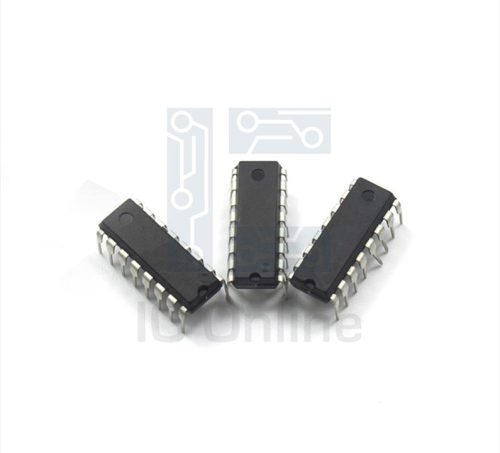
2N5114-JFET-PChannel Overview
The 2N5114 is a P-channel junction field-effect transistor (JFET) designed for low-noise and high-gain applications. Its construction enables stable operation in analog circuits that require precise voltage control and minimal signal distortion. With a maximum drain-source voltage rating suitable for many industrial environments, it offers engineers a reliable component for switching and amplification tasks. The device??s robust electrical characteristics make it a preferred choice for use in audio amplifiers, low-level signal processing, and precision analog designs. For detailed technical support and sourcing, visit IC Manufacturer.
2N5114-JFET-PChannel Key Features
- Low gate leakage current: Ensures minimal input current draw, improving signal integrity and reducing noise in sensitive analog circuits.
- High forward transfer admittance: Provides strong amplification capability, enhancing gain performance in amplifier stages.
- Wide operating voltage range: Supports drain-source voltages up to 25 V, enabling use in diverse industrial and instrumentation applications.
- Robust maximum power dissipation: Allows the device to handle up to 310 mW, increasing reliability under thermal stress and continuous operation.
2N5114-JFET-PChannel Technical Specifications
| Parameter | Value | Unit |
|---|---|---|
| Drain-Source Voltage (VDS) | -25 | V |
| Gate-Source Voltage (VGS) | -25 | V |
| Drain Current (ID) | -20 | mA |
| Gate Leakage Current (IGSS) | -100 | nA (max) |
| Forward Transfer Admittance (|Yfs|) | 2000 | ??S (min) |
| Power Dissipation (PD) | 310 | mW |
| Operating Temperature Range (TJ) | -65 to +200 | ??C |
| Package Type | TO-18 Metal Can | – |
2N5114-JFET-PChannel Advantages vs Typical Alternatives
This P-channel JFET offers superior low noise and high gain performance compared to typical transistor alternatives. Its low gate leakage current enhances sensitivity and accuracy in signal amplification, while its wide voltage and temperature tolerances improve reliability in demanding industrial environments. The device??s robust power dissipation capacity and precise electrical characteristics make it ideal for integration in analog circuits where stable, low-distortion operation is critical.
🔥 Best-Selling Products
-
Texas Instruments BQ24075 Linear Battery Charger IC – 5mm x 4mm QFN Package
-

Texas Instruments INA219 Current Sensor Module – SOIC Package, Precision Monitoring
-

Texas Instruments LM4041 Precision Voltage Reference – SOT-23 Package
-

Texas Instruments OPA2134 Audio Op Amp – Dual, High-Performance, SOIC-8 Package
Typical Applications
- Low-noise audio amplifiers requiring minimal signal distortion and high input impedance for clean sound reproduction and amplification.
- Precision analog signal processing circuits where stable gain and low leakage current are essential for accurate measurements.
- Switching applications in industrial electronics that benefit from the device??s capability to handle moderate currents and voltages efficiently.
- Sensor interface circuits that require sensitive voltage control with minimal interference for reliable data acquisition.
2N5114-JFET-PChannel Brand Info
The 2N5114 JFET is a widely recognized P-channel transistor offered by reputable semiconductor manufacturers specializing in discrete components. Known for its consistent quality and reliability, this device is packaged in a TO-18 metal can, ensuring robust mechanical protection and thermal performance. It is extensively used in industrial and instrumentation sectors due to its stable electrical performance and long-term durability.
FAQ
What is the maximum drain-source voltage rating for this JFET?
The maximum drain-source voltage (VDS) for this P-channel JFET is -25 V, meaning it can safely operate with voltages up to 25 volts applied from drain to source in the reverse polarity typical for P-channel devices.
🌟 Featured Products
-

“Buy MAX9312ECJ+ Precision Voltage Comparator in DIP Package for Reliable Performance”
-
QCC-711-1-MQFN48C-TR-03-1 Bluetooth Audio SoC with MQFN48C Package
-

0339-671-TLM-E Model – High-Performance TLM-E Package for Enhanced Functionality
-
1-1415898-4 Connector Housing, Electrical Wire-to-Board, Receptacle, Packaged
How does the low gate leakage current benefit circuit design?
Low gate leakage current reduces the input bias current in amplifier and analog circuits, resulting in improved signal integrity and lower noise levels. This makes the device ideal for sensitive signal processing where preserving signal fidelity is critical.
What package type is used for this transistor?
This JFET is housed in a TO-18 metal can package, which provides excellent thermal conductivity and mechanical protection, suitable for industrial and laboratory applications requiring stable environmental performance.
📩 Contact Us
Can this JFET handle high power dissipation in continuous operation?
Yes, with a maximum power dissipation rating of 310 mW, the device can sustain moderate power levels during continuous operation, provided adequate heat sinking or thermal management is implemented in the circuit design.
What temperature range is this device rated for?
The transistor operates reliably within a junction temperature range of -65??C to +200??C, making it suitable for a wide variety of industrial and environmental conditions without compromising performance.


