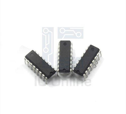
JANKCCL2N3499-Transistor-Die Overview
The JANKCCL2N3499-Transistor-Die is a high-performance semiconductor component designed for integration in advanced electronic circuits. This transistor die exhibits reliable switching and amplification capabilities, making it ideal for precision analog and digital applications. Its robust electrical characteristics support efficient power management and signal integrity, ensuring consistent performance in demanding industrial environments. Manufactured with proven semiconductor fabrication techniques, the die offers excellent thermal stability and durability. Engineers and sourcing specialists benefit from its compact form factor and compatibility with diverse packaging solutions. For more detailed product information, visit the IC Manufacturer website.
JANKCCL2N3499-Transistor-Die Key Features
- High current gain: Enables efficient signal amplification, reducing the need for additional components and simplifying circuit design.
- Low saturation voltage: Minimizes power loss during switching, enhancing overall energy efficiency in power-sensitive applications.
- Thermal stability: Maintains consistent performance under varying temperature conditions, increasing reliability in industrial environments.
- Compact die size: Facilitates integration into high-density semiconductor packages, optimizing board space utilization.
JANKCCL2N3499-Transistor-Die Technical Specifications
| Parameter | Specification |
|---|---|
| Type | NPN Transistor Die |
| Collector-Emitter Voltage (VCEO) | 60 V |
| Collector Current (IC) | 3 A |
| Power Dissipation (PD) | 1.5 W (die level) |
| Current Gain (hFE) | 100 (typical) |
| Transition Frequency (fT) | 100 MHz |
| Junction Temperature (TJ) | 150 ??C max |
| Saturation Voltage (VCE(sat)) | 0.2 V at IC = 1 A |
JANKCCL2N3499-Transistor-Die Advantages vs Typical Alternatives
This transistor die offers superior current gain and lower saturation voltage compared to typical alternatives, translating to improved signal amplification and reduced power losses. Its robust thermal tolerance enhances reliability in harsh industrial settings. Additionally, the compact die form allows flexible packaging options, enabling seamless integration into diverse circuit designs. These advantages make it a preferred choice for engineers seeking efficient, high-performance transistor solutions.
🔥 Best-Selling Products
-
Texas Instruments BQ24075 Linear Battery Charger IC – 5mm x 4mm QFN Package
-

Texas Instruments INA219 Current Sensor Module – SOIC Package, Precision Monitoring
-

Texas Instruments LM4041 Precision Voltage Reference – SOT-23 Package
-

Texas Instruments OPA2134 Audio Op Amp – Dual, High-Performance, SOIC-8 Package
Typical Applications
- Power amplification in industrial control systems requiring precise and reliable transistor performance for signal conditioning and switching tasks.
- High-frequency switching circuits where fast response and low power dissipation are critical for system efficiency.
- Embedded analog circuits demanding stable current gain under variable thermal conditions for consistent operation.
- Custom semiconductor packages in compact electronic devices needing space-efficient transistor dies for miniaturization.
JANKCCL2N3499-Transistor-Die Brand Info
The JANKCCL2N3499-Transistor-Die is produced by a reputable semiconductor manufacturer known for delivering quality bare die components suitable for industrial and commercial electronics. This product is engineered under strict quality controls to ensure high yield and reproducibility during packaging and assembly. The brand emphasizes advanced semiconductor fabrication technology, enabling the transistor die to meet stringent performance requirements across various applications. It is widely supported by detailed datasheets and technical resources for engineers and sourcing specialists.
FAQ
What type of transistor is the JANKCCL2N3499-Transistor-Die?
The transistor die is an NPN type, designed for use in amplification and switching applications. Its structural characteristics suit both analog and digital circuits where reliable performance is necessary.
🌟 Featured Products
-

“Buy MAX9312ECJ+ Precision Voltage Comparator in DIP Package for Reliable Performance”
-
QCC-711-1-MQFN48C-TR-03-1 Bluetooth Audio SoC with MQFN48C Package
-

0339-671-TLM-E Model – High-Performance TLM-E Package for Enhanced Functionality
-
1-1415898-4 Connector Housing, Electrical Wire-to-Board, Receptacle, Packaged
What is the maximum collector current supported by this transistor die?
The maximum collector current rating for this transistor die is 3 Amperes, allowing it to handle moderate power levels in various industrial electronic applications.
How does the thermal stability of this transistor die benefit circuit design?
Thermal stability ensures that the transistor??s electrical parameters remain consistent even as temperatures change, reducing the risk of performance degradation or failure in environments with fluctuating thermal conditions.
📩 Contact Us
Can this transistor die be used in high-frequency applications?
Yes, with a transition frequency of 100 MHz, the transistor die is suitable for high-frequency switching and amplification tasks, supporting efficient operation in RF and fast digital circuits.
What packaging options are compatible with the JANKCCL2N3499-Transistor-Die?
The compact die size allows it to be integrated into various semiconductor packaging formats, including custom and standard packages, enabling flexibility for designers and manufacturers in assembly processes.


