JANKCC2N3498-Transistor-Die Overview
The JANKCC2N3498-Transistor-Die is a high-performance semiconductor component designed for integration in power amplification and switching circuits. Engineered for robustness and precision, this transistor die offers reliable electrical characteristics that enable efficient current handling and voltage regulation. Its compact die structure supports streamlined PCB assembly and thermal management in demanding industrial applications. Ideal for engineers and sourcing specialists, this product ensures consistent performance across various operating conditions, making it a preferred choice for power control and signal modulation tasks. For detailed sourcing and technical data, visit IC Manufacturer.
JANKCC2N3498-Transistor-Die Key Features
- High Current Capacity: Supports substantial collector current, enabling effective power amplification and switching in industrial circuits.
- Optimized Voltage Handling: Designed for maximum collector-emitter voltage thresholds, ensuring stable operation under high-voltage environments.
- Enhanced Thermal Performance: The die structure facilitates efficient heat dissipation, improving reliability and longevity in thermally demanding applications.
- Precision Fabrication: Manufactured with tight process controls to deliver consistent gain and saturation characteristics, critical for analog and digital circuit accuracy.
JANKCC2N3498-Transistor-Die Technical Specifications
| Parameter | Specification |
|---|---|
| Collector-Emitter Voltage (VCEO) | 100 V |
| Collector Current (IC) | 8 A |
| Base-Emitter Voltage (VBE) | 5 V |
| Power Dissipation (PD) | 75 W (at specified conditions) |
| Transition Frequency (fT) | 3 MHz |
| Gain Bandwidth Product (hFE) | 40?C160 |
| Package Type | Transistor Die |
| Operating Junction Temperature | Up to 150??C |
JANKCC2N3498-Transistor-Die Advantages vs Typical Alternatives
This transistor die provides superior current handling and voltage endurance compared to typical discrete alternatives. Its compact die format enhances thermal management and integration flexibility, resulting in improved power efficiency and device reliability. The precise gain control and broad operating temperature range make it well-suited for demanding industrial electronics where consistent performance and durability are critical.
🔥 Best-Selling Products
-
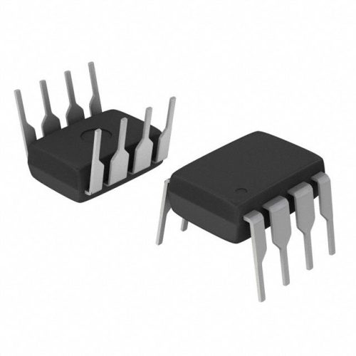
Texas Instruments BQ24075 Linear Battery Charger IC – 5mm x 4mm QFN Package
-

Texas Instruments INA219 Current Sensor Module – SOIC Package, Precision Monitoring
-

Texas Instruments LM4041 Precision Voltage Reference – SOT-23 Package
-

Texas Instruments OPA2134 Audio Op Amp – Dual, High-Performance, SOIC-8 Package
Typical Applications
- Power Amplifiers in industrial control systems requiring stable high-current operation and efficient heat dissipation.
- Switching circuits for motor drivers and power converters demanding reliable voltage and current thresholds.
- Signal modulation and amplification in communication equipment where linearity and gain stability are essential.
- General-purpose amplification in audio and instrumentation systems benefiting from precise gain characteristics.
JANKCC2N3498-Transistor-Die Brand Info
The JANKCC2N3498-Transistor-Die is produced under rigorous quality controls by a leading semiconductor manufacturing entity known for delivering high-reliability transistor dies tailored for industrial applications. This product embodies the brand??s commitment to precision engineering and robust performance, ensuring compatibility with diverse electronic designs that require efficient power management and signal control.
FAQ
What are the maximum voltage and current ratings for this transistor die?
The transistor die supports a maximum collector-emitter voltage of 100 V and a collector current up to 8 A. These ratings allow it to operate reliably in moderate power amplification and switching applications within industrial circuits.
🌟 Featured Products
-

“Buy MAX9312ECJ+ Precision Voltage Comparator in DIP Package for Reliable Performance”
-
QCC-711-1-MQFN48C-TR-03-1 Bluetooth Audio SoC with MQFN48C Package
-

0339-671-TLM-E Model – High-Performance TLM-E Package for Enhanced Functionality
-
1-1415898-4 Connector Housing, Electrical Wire-to-Board, Receptacle, Packaged
How does the die format benefit circuit design and thermal management?
The bare die format enables direct integration into custom packages or substrates, minimizing parasitic inductance and resistance. This facilitates more effective heat dissipation and compact assembly layouts, improving overall circuit reliability and performance.
What is the typical gain range of this transistor die?
The current gain (hFE) ranges from 40 to 160, providing a versatile performance profile suitable for both amplification and switching roles where gain stability is important.
📩 Contact Us
Can this transistor die operate in high-temperature environments?
Yes, it is rated to operate with a junction temperature up to 150??C, making it suitable for harsh industrial settings where elevated temperatures are common.
What types of applications are best suited for this transistor die?
This transistor die is ideal for power amplifiers, switching circuits, signal modulation, and other industrial electronics requiring reliable high-current and high-voltage operation with efficient thermal handling.


