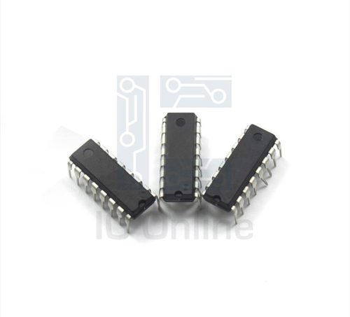
JANHCB2N3439-Transistor-Die Overview
The JANHCB2N3439-Transistor-Die is a high-performance NPN bipolar junction transistor die designed for integration into discrete or hybrid semiconductor devices. Engineered to deliver reliable switching and amplification in demanding industrial environments, this transistor die offers precise current gain and robust voltage handling capabilities. Its compact die format facilitates easy incorporation into custom assemblies, ensuring efficient thermal management and electrical performance. Ideal for engineers and sourcing specialists seeking a dependable building block for power management, signal processing, or driver circuits, this transistor die aligns with stringent quality standards from IC Manufacturer.
JANHCB2N3439-Transistor-Die Key Features
- High current gain (hFE): Ensures efficient amplification, reducing the need for additional gain stages and simplifying circuit design.
- Maximum collector-emitter voltage: Supports robust voltage handling, enabling use in high-voltage switching and power regulation applications.
- Low saturation voltage: Minimizes power loss during conduction, improving overall system efficiency and thermal performance.
- Die format: Allows for easy integration into hybrid modules or custom packaging, enhancing flexibility for system designers.
JANHCB2N3439-Transistor-Die Technical Specifications
| Parameter | Value | Unit |
|---|---|---|
| Collector-Emitter Voltage (VCEO) | 40 | V |
| Collector Current (IC) | 5 | A |
| Gain Bandwidth Product (fT) | 100 | MHz |
| DC Current Gain (hFE) | 100?C320 | ?C |
| Collector Dissipation (PC) | 1 | W |
| Junction Temperature (Tj) | 150 | ??C |
| Emitter-Base Voltage (VEBO) | 5 | V |
| Package Type | Die | ?C |
JANHCB2N3439-Transistor-Die Advantages vs Typical Alternatives
This transistor die offers superior integration flexibility compared to packaged transistors, enabling tailored hybrid assemblies with optimized thermal and electrical performance. Its high current gain and low saturation voltage contribute to enhanced power efficiency and switching accuracy. Additionally, the robust voltage ratings and reliable junction temperature tolerance make it a dependable choice over standard discrete transistors in industrial semiconductor applications.
🔥 Best-Selling Products
-
Texas Instruments BQ24075 Linear Battery Charger IC – 5mm x 4mm QFN Package
-

Texas Instruments INA219 Current Sensor Module – SOIC Package, Precision Monitoring
-

Texas Instruments LM4041 Precision Voltage Reference – SOT-23 Package
-

Texas Instruments OPA2134 Audio Op Amp – Dual, High-Performance, SOIC-8 Package
Typical Applications
- Power amplification stages in industrial control systems requiring reliable current handling and signal integrity.
- Switching circuits in power management modules for efficient energy conversion and load control.
- Driver stages for motors and relays where precise switching and durability are critical.
- Hybrid integrated circuits where compact transistor dies support miniaturization and performance optimization.
JANHCB2N3439-Transistor-Die Brand Info
This transistor die is supplied by a leading semiconductor manufacturer known for stringent quality control and advanced fabrication technologies. The brand specializes in high-reliability components for industrial and commercial applications, ensuring that each die meets rigorous electrical and thermal specifications. This product exemplifies the brand??s commitment to performance consistency and integration readiness in demanding electronic systems.
FAQ
What is the maximum collector current rating for this transistor die?
The maximum collector current rating is 5 amperes, allowing the die to handle moderate power levels suitable for many industrial switching and amplification applications.
🌟 Featured Products
-

“Buy MAX9312ECJ+ Precision Voltage Comparator in DIP Package for Reliable Performance”
-
QCC-711-1-MQFN48C-TR-03-1 Bluetooth Audio SoC with MQFN48C Package
-

0339-671-TLM-E Model – High-Performance TLM-E Package for Enhanced Functionality
-
1-1415898-4 Connector Housing, Electrical Wire-to-Board, Receptacle, Packaged
Can this transistor die operate at high frequencies?
Yes, with a gain bandwidth product of approximately 100 MHz, this transistor die supports high-frequency operation compatible with signal processing and fast switching requirements.
How does the die format benefit system designers?
The bare die format allows engineers to integrate the transistor directly into hybrid modules or custom packages, providing enhanced thermal management and reducing parasitic effects compared to standard packaged transistors.
📩 Contact Us
What voltage levels can the transistor die withstand?
The collector-emitter voltage rating is 40 volts, while the emitter-base voltage is rated at 5 volts, ensuring reliable operation within typical industrial voltage ranges.
Is thermal management a concern when using this transistor die?
While the die supports junction temperatures up to 150??C, proper heat dissipation strategies such as heat sinks or thermal interface materials are recommended to maintain optimal performance and longevity.


