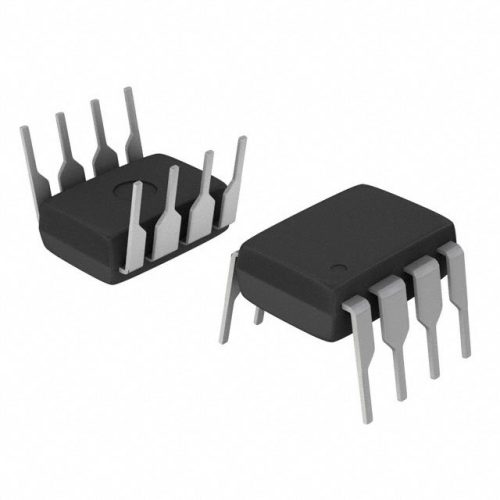
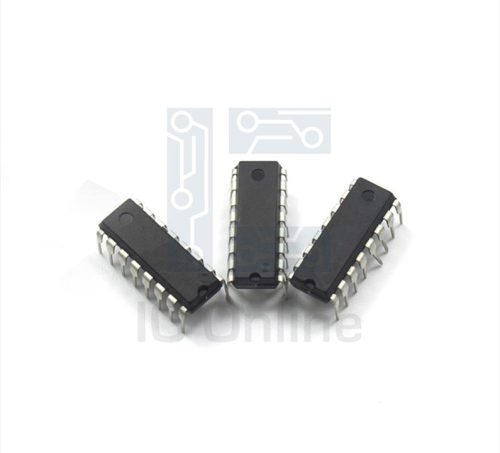
JANSE2N3700-Transistor Overview
The JANSE2N3700 transistor is a robust NPN bipolar junction transistor designed for general-purpose amplification and switching applications. It features a durable silicon structure that supports moderate voltage and current levels, making it suitable for industrial and consumer electronics. The device offers reliable performance with a collector-emitter voltage rating of up to 60V and collector current capacity of 200mA. Its design ensures efficient switching with a gain bandwidth product that supports a wide range of signal frequencies. This transistor is well-suited for engineers and sourcing specialists seeking a dependable component for medium power stages. For more technical resources, visit IC Manufacturer.
JANSE2N3700-Transistor Key Features
- High voltage tolerance: Supports collector-emitter voltage up to 60V, enabling use in circuits with moderate voltage requirements.
- Moderate current handling: Can manage collector current up to 200mA, suitable for driving small loads or amplification tasks.
- Reliable gain performance: Provides a DC current gain (hFE) range that ensures consistent amplification across various operating conditions.
- Fast switching capabilities: Low switching times reduce delay in signal transitions, enhancing efficiency in switching circuits.
JANSE2N3700-Transistor Technical Specifications
| Parameter | Symbol | Value | Unit |
|---|---|---|---|
| Collector-Emitter Voltage | VCEO | 60 | V |
| Collector-Base Voltage | VCBO | 75 | V |
| Emitter-Base Voltage | VEBO | 5 | V |
| Collector Current | IC | 200 | mA |
| Power Dissipation | Ptot | 625 | mW |
| DC Current Gain (hFE) | hFE | 40?C300 | (typical) |
| Transition Frequency | fT | 40 | MHz |
| Operating Temperature Range | Top | -55 to +150 | ??C |
JANSE2N3700-Transistor Advantages vs Typical Alternatives
This transistor offers a balanced combination of voltage tolerance and current capacity, making it more versatile than many low-power transistors. Its moderate power dissipation and wide gain range ensure stable operation in switching and amplification roles. Compared to typical alternatives, it supports faster switching speeds with reliable thermal performance, reducing circuit losses and improving overall system efficiency.
🔥 Best-Selling Products
Typical Applications
- Signal amplification in audio and low-frequency circuits, where consistent gain and low distortion are critical for performance.
- Switching applications in power control systems, enabling efficient control of loads up to 200mA.
- Driver stages for relays and small motors, providing sufficient current and voltage handling capabilities.
- General purpose electronic circuits including sensor interfaces and digital logic level translation.
JANSE2N3700-Transistor Brand Info
The JANSE2N3700 transistor is manufactured by a reputable semiconductor company known for producing reliable, industrial-grade electronic components. This product line emphasizes consistent quality and adherence to stringent manufacturing standards, ensuring dependable performance in various demanding environments. The transistor is widely adopted in both legacy and modern designs due to its proven track record and broad availability.
FAQ
What is the maximum voltage rating of this transistor?
The maximum voltage rating between collector and emitter (VCEO) is 60 volts, which defines the highest voltage the transistor can safely handle in typical circuit configurations without breakdown.
🌟 Featured Products
-

“Buy MAX9312ECJ+ Precision Voltage Comparator in DIP Package for Reliable Performance”
-
QCC-711-1-MQFN48C-TR-03-1 Bluetooth Audio SoC with MQFN48C Package
-

0339-671-TLM-E Model – High-Performance TLM-E Package for Enhanced Functionality
-
1-1415898-4 Connector Housing, Electrical Wire-to-Board, Receptacle, Packaged
Can this transistor handle high-frequency signals?
Yes, with a transition frequency (fT) of around 40 MHz, it is capable of switching and amplifying signals at moderate frequencies, making it suitable for many analog and digital applications.
What is the typical current gain range for this device?
The DC current gain (hFE) typically ranges from 40 to 300, allowing flexibility in amplification levels depending on the operating conditions and circuit design.
📩 Contact Us
Is this transistor suitable for power switching applications?
While it supports collector currents up to 200mA and power dissipation of 625mW, it is best suited for low to medium power switching rather than high power loads.
What temperature range can this transistor operate within?
The device is rated for an operating temperature range from -55??C to +150??C, ensuring stable performance across a wide range of industrial and environmental conditions.


