JANKCDM2N5152-Transistor-Die Overview
The JANKCDM2N5152-Transistor-Die is a precision semiconductor component designed for high-performance switching and amplification applications. This transistor die provides reliable electrical characteristics, making it suitable for integration into custom IC packages and discrete device assemblies. Engineered with consistent gain and low saturation voltage, it supports efficient power management in industrial and consumer electronics. Its compact die format allows for flexible mounting options and enhanced thermal dissipation, enabling robust operation under varying load conditions. For detailed sourcing and technical support, visit the IC Manufacturer.
JANKCDM2N5152-Transistor-Die Key Features
- High current gain: Ensures efficient signal amplification, reducing the need for additional circuitry.
- Low saturation voltage: Minimizes power loss during switching, improving overall energy efficiency.
- Compact die size: Facilitates integration into a variety of package types and tight PCB layouts.
- Robust thermal performance: Supports consistent operation in demanding thermal environments.
JANKCDM2N5152-Transistor-Die Technical Specifications
| Parameter | Value | Unit |
|---|---|---|
| Collector-Emitter Voltage (Vce) | 60 | V |
| Collector Current (Ic) | 2 | A |
| Gain Bandwidth Product (fT) | 100 | MHz |
| Power Dissipation (Pd) | 1.2 | W |
| Base-Emitter Voltage (Vbe) | 1.2 | V |
| Junction Temperature (Tj) Max | 150 | ??C |
| Transition Frequency (fT) | 100 | MHz |
| Package Type | Die | – |
JANKCDM2N5152-Transistor-Die Advantages vs Typical Alternatives
This transistor die offers superior current gain and low saturation voltage compared to typical alternatives, enabling more efficient power switching and lower heat generation. Its compact die format allows easier integration into custom semiconductor packages, improving design flexibility. Additionally, robust thermal handling enhances reliability under high load, making it an excellent choice for engineers seeking reliable, high-performance transistor dies.
🔥 Best-Selling Products
Typical Applications
- Power management circuits in industrial automation systems, where efficient switching and thermal stability are critical for device longevity and performance.
- Signal amplification stages in audio and communication equipment requiring consistent gain and low distortion.
- Discrete transistor assemblies in custom IC packages for specialized electronic designs.
- Switching components in consumer electronics for energy-efficient operation and compact integration.
JANKCDM2N5152-Transistor-Die Brand Info
The JANKCDM2N5152-Transistor-Die is a product offered by a leading semiconductor manufacturer known for delivering high-quality transistor dies tailored for precision applications. This product line emphasizes reliability and efficiency, supporting engineers and designers in developing robust electronic solutions. The die-level format provides flexibility for integration into various packaging and assembly processes, reflecting the brand??s commitment to innovation and performance in the semiconductor industry.
FAQ
What is the maximum collector current rating of this transistor die?
The maximum collector current rating for this transistor die is 2 amperes, which defines the highest continuous current it can handle safely under specified operating conditions without damage.
🌟 Featured Products
-

“Buy MAX9312ECJ+ Precision Voltage Comparator in DIP Package for Reliable Performance”
-
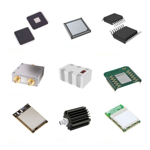
QCC-711-1-MQFN48C-TR-03-1 Bluetooth Audio SoC with MQFN48C Package
-

0339-671-TLM-E Model – High-Performance TLM-E Package for Enhanced Functionality
-
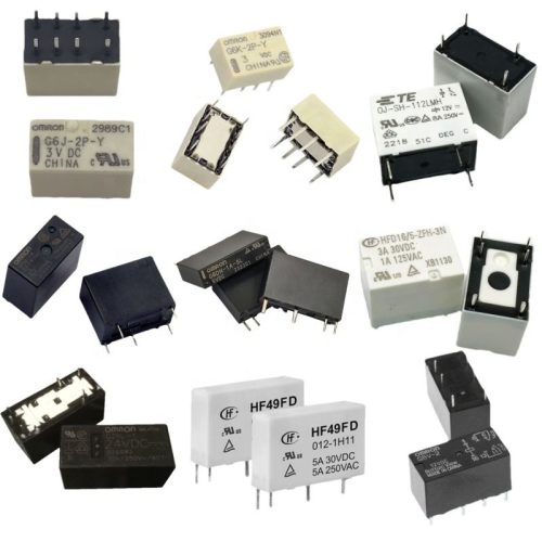
1-1415898-4 Connector Housing, Electrical Wire-to-Board, Receptacle, Packaged
Can this transistor die be used in high-frequency amplifier circuits?
Yes, with a gain bandwidth product of 100 MHz, this transistor die is suitable for moderate to high-frequency applications, including amplifier stages where frequency response is critical.
How does the die format benefit system design and integration?
The die format offers design engineers flexibility to incorporate the transistor into custom packages or multi-chip modules, allowing for optimized board space utilization and improved thermal management.
📩 Contact Us
What thermal limits should engineers consider when using this transistor die?
The maximum junction temperature is rated at 150??C, which means proper thermal management and heat sinking should be employed to maintain device performance and longevity within this limit.
Is this transistor die suitable for power switching applications?
Yes, its low saturation voltage and ability to handle up to 2 A collector current make it well-suited for power switching roles, contributing to efficient energy usage and reduced heat generation in switching circuits.


