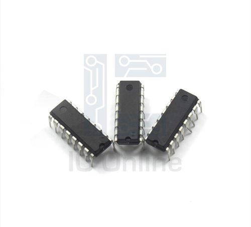
MQ2N4856-JFET-NChannel Overview
The MQ2N4856-JFET-NChannel is a precision N-channel junction field-effect transistor (JFET) designed for low-noise, high-input-impedance applications. It offers stable electrical characteristics and reliable performance under varied operating conditions, making it ideal for analog signal processing and low-level amplification tasks. This device features a robust construction optimized for consistent switching and low gate leakage current. Engineers and sourcing specialists can leverage this transistor for applications demanding high gain, low distortion, and efficient integration. For detailed specifications and purchasing, visit IC Manufacturer.
MQ2N4856-JFET-NChannel Key Features
- Low Noise Performance: Enables superior signal integrity in sensitive analog circuits, reducing unwanted interference and improving accuracy.
- High Input Impedance: Minimizes loading effects on preceding stages, preserving signal fidelity and enhancing overall circuit performance.
- Stable Operating Parameters: Ensures reliable function over temperature variations and voltage fluctuations, enhancing device longevity and robustness.
- Compact TO-92 Package: Facilitates easy integration into compact circuit boards while maintaining effective thermal dissipation.
MQ2N4856-JFET-NChannel Technical Specifications
| Parameter | Value | Unit |
|---|---|---|
| Drain-Source Voltage (VDS) | 30 | V |
| Gate-Source Voltage (VGS) | ??20 | V |
| Drain Current (ID) | 10 | mA |
| Gate Cutoff Voltage (VGS(off)) | -0.5 to -4.0 | V |
| Forward Transfer Admittance (|Yfs|) | 5 | mS |
| Input Capacitance (Ciss) | 4 | pF |
| Noise Figure | Low | ?? |
| Operating Temperature Range | -55 to +150 | ??C |
MQ2N4856-JFET-NChannel Advantages vs Typical Alternatives
This N-channel JFET offers enhanced sensitivity and low noise characteristics compared to typical bipolar transistors or MOSFETs used in similar roles. Its high input impedance reduces signal loss, while the stable gate cutoff voltage ensures consistent switching behavior. These factors contribute to improved accuracy and reliability in analog circuits, making it a preferred choice for precision amplification and switching applications.
🔥 Best-Selling Products
-
Texas Instruments BQ24075 Linear Battery Charger IC – 5mm x 4mm QFN Package
-

Texas Instruments INA219 Current Sensor Module – SOIC Package, Precision Monitoring
-

Texas Instruments LM4041 Precision Voltage Reference – SOT-23 Package
-

Texas Instruments OPA2134 Audio Op Amp – Dual, High-Performance, SOIC-8 Package
Typical Applications
- Low-noise preamplifiers in audio and instrumentation systems, where preserving signal clarity and minimizing distortion are critical.
- Analog switches and choppers requiring fast, stable switching with minimal leakage current.
- Buffer stages in sensor interfaces, enhancing signal integrity from high-impedance sources.
- Voltage-controlled resistors and amplifiers in analog signal processing circuits demanding linear response.
MQ2N4856-JFET-NChannel Brand Info
The MQ2N4856-JFET-NChannel is manufactured by a reputable semiconductor supplier recognized for delivering high-quality discrete components tailored for industrial and professional electronics. This product line is engineered to meet stringent performance standards, ensuring dependable operation in demanding environments. Its consistent manufacturing process and rigorous quality control underline its suitability for critical applications where precision and reliability are paramount.
FAQ
What is the maximum drain-source voltage rating for this JFET?
The maximum drain-source voltage (VDS) for the MQ2N4856-JFET-NChannel is specified at 30 volts. This voltage rating indicates the highest voltage the device can safely handle between the drain and source terminals without breakdown.
🌟 Featured Products
-

“Buy MAX9312ECJ+ Precision Voltage Comparator in DIP Package for Reliable Performance”
-
QCC-711-1-MQFN48C-TR-03-1 Bluetooth Audio SoC with MQFN48C Package
-

0339-671-TLM-E Model – High-Performance TLM-E Package for Enhanced Functionality
-
1-1415898-4 Connector Housing, Electrical Wire-to-Board, Receptacle, Packaged
How does the gate cutoff voltage affect device operation?
The gate cutoff voltage (VGS(off)) defines the gate-to-source voltage at which the transistor stops conducting. For this device, it ranges from -0.5 V to -4.0 V, allowing precise control of current flow and enabling its use in switching and amplification with predictable threshold behavior.
What is the significance of the high input impedance feature?
High input impedance minimizes the current drawn from preceding circuit stages, which prevents signal degradation and loading effects. This is particularly important in sensor and low-level signal applications where maintaining signal integrity is critical.
📩 Contact Us
Can this JFET operate reliably over a wide temperature range?
Yes, the device is rated for operation from -55??C up to +150??C, making it suitable for industrial and harsh environment applications where temperature stability and reliability are required.
Is the MQ2N4856 suitable for audio frequency amplification?
Absolutely. Its low noise figure and stable gain characteristics make it well-suited for audio frequency amplification, ensuring clean signal amplification with minimal distortion or interference.


